- 您现在的位置:买卖IC网 > Sheet目录1992 > CY28410OXC-2 (Silicon Laboratories Inc)IC CLOCK CK410 GRANTSDALE 56SSOP
CY28410-2
......................Document #: 38-07747 Rev *.* Page 14 of 16
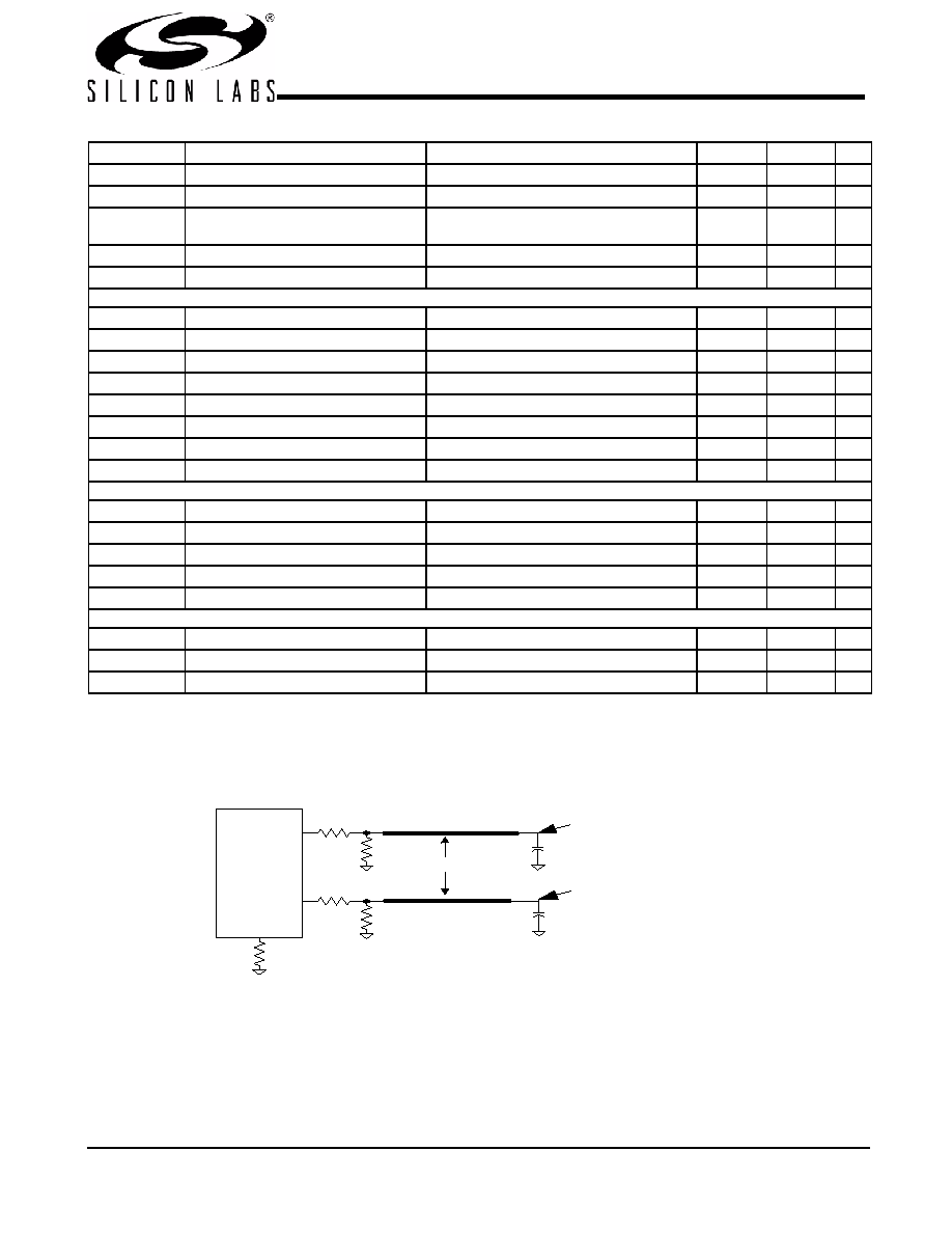
Test and Measurement Set-up
For Differential CPU, SRC and DOT96 Output Signals
The following diagram shows the test load configuration for the
differential CPU and SRC outputs.
VLOW
Voltage Low
Math averages Figure 7
–150
–
mV
VOX
Crossing Point Voltage at 0.7V Swing
250
550
mV
VOVS
Maximum Overshoot Voltage
–
VHIGH +
0.3
V
VUDS
Minimum Undershoot Voltage
–0.3
–
V
VRB
Ring Back Voltage
See Figure 7. Measure SE
–
0.2
V
USB
TDC
Duty Cycle
Measurement at 1.5V
45
55
%
TPERIOD
Period
Measurement at 1.5V
20.83125 20.83542
ns
TPERIODAbs
Absolute Period
Measurement at 1.5V
20.48125 21.18542
ns
THIGH
USB high time
Measurement at 2.4V
8.094
10.036
ns
TLOW
USB low time
Measurement at 0.4V
7.694
9.836
ns
TR / TF
Rise and Fall Times
Measured between 0.8V and 2.0V
0.475
1.4
ns
TCCJ
Cycle to Cycle Jitter
Measurement at 1.5V
–
350
ps
LACC
USB Long Term Accuracy
–
100
ppm
REF
TDC
REF Duty Cycle
Measurement at 1.5V
45
55
%
TPERIOD
REF Period
Measurement at 1.5V
69.8203
69.8622
ns
TPERIODAbs
REF Absolute Period
Measurement at 1.5V
68.82033 70.86224
ns
TR / TF
REF Rise and Fall Times
Measured between 0.8V and 2.0V
0.35
2.0
V/ns
TCCJ
REF Cycle to Cycle Jitter
Measurement at 1.5V
–
1000
ps
ENABLE/DISABLE and SET-UP
TSTABLE
Clock Stabilization from Power-up
–
1.8
ms
TSS
Stopclock Set-up Time
10.0
–
ns
TSH
Stopclock Hold Time
0
–
ns
AC Electrical Specifications (continued)
Parameter
Description
Condition
Min.
Max.
Unit
CPU T
CP UC
M e a s ur em en t
Po in t
2p F
IR E F
M e a s ur em e n t
Po in t
2p F
S RCT
S RCC
D iffe re n tia l
D O T 96T
DO T 9 6 C
Figure 7. 0.7V Single-ended Load Configuration
发布紧急采购,3分钟左右您将得到回复。
相关PDF资料
CY28410OXC
IC CLOCK CK410 GRANTSDALE 56SSOP
CY28411ZXC
IC CLOCK CK410M ALVISO 56TSSOP
CY28442ZXC-2
IC CLOCK ALVISO PENTM 56TSSOP
CY28445LFXC-5
IC CLOCK CALISTOGA CK410M 68QFN
CY28446LFXC
IC CLOCK CALISTOGA CK410M 64QFN
CY28447LFXC
IC CLOCK CALISTOGA CK410M 72QFN
CY28547LFXCT
IC CLOCK CK505/410M INTEL 72QFN
CY28548ZXC
IC CLK CK505 960M/965M 64TSSOP
相关代理商/技术参数
CY28410OXC-2T
功能描述:时钟发生器及支持产品 SysClk Intel Lakeprt & Grantsdale Chipset RoHS:否 制造商:Silicon Labs 类型:Clock Generators 最大输入频率:14.318 MHz 最大输出频率:166 MHz 输出端数量:16 占空比 - 最大:55 % 工作电源电压:3.3 V 工作电源电流:1 mA 最大工作温度:+ 85 C 安装风格:SMD/SMT 封装 / 箱体:QFN-56
CY28410OXCT
功能描述:时钟发生器及支持产品 SysClk Intel Lakeprt & Grantsdale Chipset RoHS:否 制造商:Silicon Labs 类型:Clock Generators 最大输入频率:14.318 MHz 最大输出频率:166 MHz 输出端数量:16 占空比 - 最大:55 % 工作电源电压:3.3 V 工作电源电流:1 mA 最大工作温度:+ 85 C 安装风格:SMD/SMT 封装 / 箱体:QFN-56
CY28410ZC
制造商:SPECTRALINEAR 制造商全称:SPECTRALINEAR 功能描述:Clock Generator for Intel Grantsdale Chipset
CY28410ZCT
制造商:SPECTRALINEAR 制造商全称:SPECTRALINEAR 功能描述:Clock Generator for Intel Grantsdale Chipset
CY28410ZXC
功能描述:时钟发生器及支持产品 SysClk Intel Lakeprt & Grantsdale Chipset RoHS:否 制造商:Silicon Labs 类型:Clock Generators 最大输入频率:14.318 MHz 最大输出频率:166 MHz 输出端数量:16 占空比 - 最大:55 % 工作电源电压:3.3 V 工作电源电流:1 mA 最大工作温度:+ 85 C 安装风格:SMD/SMT 封装 / 箱体:QFN-56
CY28410ZXC-2
制造商:CYPRESS 制造商全称:Cypress Semiconductor 功能描述:Clock Generator for Intel Grantsdale Chipset
CY28410ZXC-2T
制造商:CYPRESS 制造商全称:Cypress Semiconductor 功能描述:Clock Generator for Intel Grantsdale Chipset
CY28410ZXCT
功能描述:时钟发生器及支持产品 SysClk Intel Lakeprt & Grantsdale Chipset RoHS:否 制造商:Silicon Labs 类型:Clock Generators 最大输入频率:14.318 MHz 最大输出频率:166 MHz 输出端数量:16 占空比 - 最大:55 % 工作电源电压:3.3 V 工作电源电流:1 mA 最大工作温度:+ 85 C 安装风格:SMD/SMT 封装 / 箱体:QFN-56